We, 26.8.2026 | Original article from: LabRulezICPMS Library
This week we bring you application notes by Agilent Technologies, Shimadzu, Thermo Fisher Scientific and Waters Corporation!News from LabRulezICPMS Library - Week 35, 2026
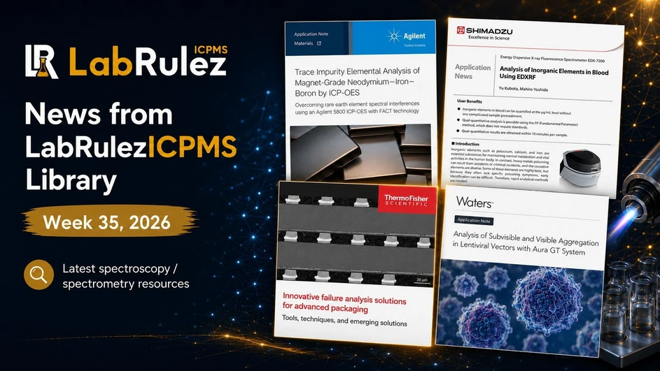
LabRulez / AI: News from LabRulezICPMS Library - Week 35, 2026
Our Library never stops expanding. What are the most recent contributions to LabRulezICPMS Library in the week of 24th August 2026? Check out new documents from the field of spectroscopy/spectrometry and related techniques!
👉 SEARCH THE LARGEST REPOSITORY OF DOCUMENTS ABOUT SPECTROSCOPY/SPECTROMETRY RELATED TECHNIQUES
👉 Need info about different analytical techniques? Peek into LabRulezLCMS or LabRulezGCMS libraries.
This week we bring you application notes by Agilent Technologies, Shimadzu, Thermo Fisher Scientific and Waters Corporation!
1. Agilent Technologies: Trace Impurity Elemental Analysis of Magnet-Grade Neodymium–Iron– Boron by ICP-OES
Overcoming rare earth element spectral interferences using an Agilent 5800 ICP-OES with FACT technology
- Application note
- Full PDF for download
Neodymium (NdFeB) magnets are high-performance permanent magnetic materials that are widely used in electric vehicles, wind power, electronics, aerospace, and other industries. NdFeB is a key foundational material supporting energy conservation, environmental protection, advanced manufacturing, and many other emerging industries. Its performance directly affects the energy efficiency and value of final products.
The main magnetic phase of NdFeB is Nd2 Fe14B. Minor elements and impurities, including rare earth elements (REEs) such as praseodymium (Pr), samarium (Sm), dysprosium (Dy), and gadolinium (Gd) can disrupt the crystal structure of the main phase through atomic substitution, resulting in possible degradation of magnetic performance. Fluctuations in impurity element content can also interfere with critical processes such as melting and sintering, leading to a sharp decline in product yield. Accurate quantification of REE impurities in NdFeB is therefore essential.
China has published seven standardized chemical analysis methods for NdFeB alloys, which cover REEs and impurities. Part II of the Chemical Analysis Methods for Neodymium– Iron–Boron Alloys (XB/T 617)1 series uses inductively coupled plasma optical emission spectrometry (ICP-OES). However, during testing by ICP-OES, REEs produce numerous emission lines at closely spaced wavelengths, making them highly susceptible to spectral interference. If left unchecked, these interferences would compromise the accuracy of the quantitative results for REEs in NdFeB.
This study presents a method for the Agilent 5800 ICP-OES that uses proprietary Fast Automated Curve-fitting Technique (FACT) background correction to eliminate spectral interferences between REEs.2 This method improves the accuracy and detection limits for 13 REEs in NdFeB, providing efficient quality control (QC) of NdFeB materials.
Experimental
Instrumentation An Agilent 5800 ICP-OES equipped with a SeaSpray nebulizer, double-pass cyclonic spray chamber, and a fully demountable torch assembly with a 1.8 mm inner diameter injector was used. The instrument was controlled using Agilent ICP Expert software (version 7.7.3). Instrument operating parameters are summarized in Table 1. The software includes FACT, comprehensive QC, and IntelliQuant semiquantitative analysis that provides five-star spectral line recommendations, interference diagnostics, and data screening functions (Figure 1).
Conclusion
An Agilent 5800 ICP-OES combined with Agilent Fast Automated Curve-fitting Technique (FACT) background correction was used successfully to analyze 13 rare earth element (REE) impurity elements in an NdFeB sample. Instrument detection limits for all elements were below 5 ppb, demonstrating the high sensitivity of the 5800 ICP-OES. Despite the complexity of rare-earth impurity analysis in NdFeB materials, FACT effectively eliminated spectral interferences between the REEs, enabling spike recoveries of 90 to 111% for all 13 elements. These results confirm that the method provides excellent sensitivity and accuracy, making it well suited for the quantitative determination of REE impurities in NdFeB materials.
2. Shimadzu: Analysis of Inorganic Elements in Blood Using EDXRF
- Application note
- Full PDF for download
User benefits
- Inorganic elements in blood can be quantified at the µg/mL level without any complicated sample pretreatment.
- Qual-quantitative analysis is possible using the FP (Fundamental Parameter) method, which does not require standards.
- Qual-quantitative results are obtained within 10 minutes per sample.
Inorganic elements such as potassium, calcium, and iron are essential substancesfor maintaining normal metabolism and vital activities in the human body. In contrast, heavy metals poisoning can result from accidents or criminal incidents, and the causative elements are diverse. Some of these elements are highly toxic, but because they often lack specific poisoning symptoms, early identification can be difficult. Therefore, rapid analytical methods are needed.
Inorganic elements are generally analyzed by ICP-AES or ICP-MS. Although these techniques allow trace-level quantitation, they require chemical pretreatment such as dilution and deproteinization, and the samples are limited to liquids. In contrast, EDX-7200 enables simple, non-destructive analysis in a short time and has sufficientsensitivity forscreening purpose. This application describes quantitative analysis results for 15 elements in blood using calibration curves, and qualitative and quantitative analysis results using the FP method based on sensitivity coefficients built into the instrument. The accuracy of the quantitative values obtained by the FP method was 84–103%, demonstrating sufficient quantitative performance. Analysis can be completed within 10 minutes persample.
Conclusion
The FP method demonstrated high accuracy for quantitation without calibration curves. In addition, blood samples do not require complicated pretreatment such as deproteinization, and the analysis time is only about 10 minutes.
3. Thermo Fisher Scientific: Innovative failure analysis solutions for advanced packaging
Tools, techniques, and emerging solutions
- Application note
- Full PDF for download
As semiconductor technology advances, the demand for high-performance, power-efficient, and miniaturized devices is rapidly growing. Advanced packaging technologies, such as 2.5D, 3D integration, wafer-level packaging (WLP), and heterogeneous integration, play a crucial role in enabling these innovations. However, as packaging structures become more complex, new reliability challenges and failure mechanisms emerge, necessitating sophisticated failure analysis (FA) methodologies. FA is critical for identifying defects, improving yield, ensuring product reliability, and reducing time-to-market for semiconductor manufacturers.
This white paper explores the evolving landscape of FA in advanced packaging, detailing the most common failure mechanisms, including interconnect degradation, delamination, electromigration, and thermal-induced stress. It examines cutting-edge FA techniques—both non-destructive and destructive—such as X-ray computed tomography (XCT), scanning acoustic microscopy (SAM), lock-in thermography (LIT), focused ion beam (FIB) analysis, and transmission electron microscopy (TEM).
Despite advancements in FA tools, the miniaturization of semiconductor devices presents new challenges, such as limited accessibility to buried interconnects, complex material interactions, and increased failure mode variability. The industry is responding by developing real-time monitoring techniques, high-resolution imaging solutions, and advanced simulation models to enhance reliability assessments.
Through case studies and industry insights, this white paper highlights the best practices for FA in advanced packaging, and it outlines future directions for the field. As semiconductor packaging continues to evolve, a proactive approach to FA will be essential in ensuring product quality, optimizing manufacturing processes, and driving innovation in next-generation electronic devices.
Key technologies under the advanced packaging umbrella:
- Fan-out wafer-level packaging (FOWLP)— Used in mobile and AI processors.
- 2.5D packaging—Uses a silicon interposer for high-bandwidth memory (HBM) integration.
- 3D integration—Uses through-silicon vias (TSVs) to stack logic and memory dies.
- Chiplet architectures—Modular approach enabling higher yield and cost efficiency.
Failure analysis techniques for advanced packaging
Non-destructive techniques
X-ray computed tomography
XCT is a non-destructive imaging technique used in semiconductor packaging to inspect internal structures, detect defects, and analyze material properties. It enables 3D visualization of complex packaging architectures, including TSVs, microbumps, RDLs, and underfill voids, without requiring physical cross-sectioning. Key applications include solder joint inspection, HB failure detection, and void analysis in FOWLP, 2.5D interposers, and 3D ICs 38. Engineers use micro-CT (~1 µm resolution), nano-CT (~50 nm resolution), and dual-energy XCT to analyze defects, differentiate materials, and optimize manufacturing39. While versatile, XCT struggles with high-density logic chips at ≤5 nm nodes 40.
Resolution varies: Micro-CT for package inspection, nano-CT for interconnect defects, and dual-energy XCT for material differentiation 41. However, high-density semiconductor devices pose several challenges. Advanced logic chips (e.g., 5 nm and below) contain ultra-fine interconnects and dense metal layers that strongly absorb X-rays, causing image artifacts and limiting penetration 42. Additionally, beam hardening effects, diffraction-induced distortions, and poor contrast in low-Z materials (e.g., polymers, oxides) make it difficult to accurately analyze deep-layer structures 43. The trade-off between scan time and resolution is another challenge. While high-resolution nano-CT scans provide better detail, they can take over an hour per sample, making them impractical for high-volume manufacturing (HVM) defect detection 44. Therefore, while XCT is highly effective for package-level defect inspection (TSVs, solder joints, and voids), it is not suitable for sub-10 nm interconnect analysis in highdensity logic chips, where techniques like TEM, SEM, and FIB remain essential for nanoscale defect characterization 45.
Scanning acoustic microscopy
SAM is a non-destructive ultrasonic imaging technique used in semiconductor packaging to detect internal defects such as delamination, voids, cracks, and adhesion failures within multi-layered structures. SAM operates by transmitting highfrequency ultrasound waves (typically in the MHz to GHz range) into the sample. These waves interact with different material layers and interfaces, where they undergo reflection, refraction, and scattering based on the acoustic impedance differences between materials. A piezoelectric transducer detects the returning echoes, which are processed to generate highresolution images of the internal structure of the package.
Destructive techniques
DualBeam FIB-SEM microscopy
DualBeam™ FIB-SEM involves using a focused beam of ions (usually gallium ions) to interact with a sample surface, which is then analyzed by SEM. FIB-SEM combines two distinct techniques. With FIB, the ion beam can mill (remove material) or modify the surface of the sample. It is highly focused and can be used for deposition, precision cutting, imaging, and analysis. This makes it very useful for applications that require micro- or nanoscale precision. SEM detects secondary electrons emitted from the sample when it is bombarded by the ion beam, creating high-resolution 2D images. This provides high spatial resolution for surface morphology and elemental analysis via energy-dispersive X-ray spectroscopy (EDS) and the characterizations of crystalline orientation and phase distribution via electron backscatter diffraction (EBSD).
The working principle of DualBeam FIB-SEM is for the ion beam to mill away layers of the material in a controlled manner. As the ion beam interacts with the sample, it causes sputtering, where atoms or ions are ejected from the sample’s surface. The SEM simultaneously captures high-resolution images of the exposed cross-sections, allowing for detailed imaging of internal structures. The combination of milling and imaging enables precise 3D reconstruction and analysis of the material’s internal layers, which is critical for advanced packaging in semiconductor devices, such as assessing vias, interconnects, and microstructures.
Summary
Advanced packaging failure analysis presents numerous challenges due to the increasing complexity and miniaturization of semiconductor devices. The transition to heterogeneous integration and 3D packaging has introduced significant benefits in performance and power efficiency but also presents new challenges related to manufacturing defects, interconnect reliability, and material integrity. Addressing these issues requires advanced metrology techniques, rigorous quality control, and improved material engineering. As semiconductor technology continues to evolve, AI-driven defect analysis and real-time monitoring will play a critical role in improving yield and reliability.
Building a comprehensive failure analysis workflow involves integrating various state-of-the-art tools and techniques to cover all stages of the manufacturing process, from wafer to die to device level. We have organized a comprehensive solution that addresses these complexities, offering a suite of advanced instruments and software tailored for the needs of the advanced packaging industry. At the wafer level, our ELITE System provides high-throughput inspection, helping to ensure early detection of defects. Transitioning to the die level, the Apreo ChemiSEM System combines high-resolution imaging with rapid elemental analysis, enabling precise identification of material compositions and contaminants. For localized and detailed analysis, the Helios 5 Hydra FIB-SEM excels in site-specific cross-sectioning and 3D imaging, while the Talos (S)TEM offers atomic-level resolution for detailed structural analysis.
To streamline and enhance the failure analysis process, we also offer automated Thermo Scientific software solutions such as AutoTEM™, iFast, and Avizo Software. AutoTEM Software automates the preparation of TEM samples, significantly reducing the time and effort required for high-precision analysis. iFast Software enables automated workflows for FIB-SEMs, improving efficiency and consistency in sample preparation and analysis. Avizo Software provides advanced visualization and analysis tools, integrating data from various sources to create comprehensive 3D models and facilitating a deeper understanding of failure mechanisms. These automated solutions not only enhance the accuracy and efficiency of failure analysis but also cater to versatile requests from customers, helping to ensure that their specific needs are met with precision and reliability.
By leveraging the combined power of our advanced instruments and automated software solutions, we offer a comprehensive, exceptional failure analysis workflow that addresses the intricate challenges of advanced packaging. This integrated approach helps identify and characterize defects with remarkable accuracy and efficiency, driving continuous improvement in packaging reliability and performance. Our total solution, encompassing electrical and physical failure analysis, provides the versatility and precision required to meet the evolving demands of the advanced packaging industry
4. Waters Corporation: Analysis of Subvisible and Visible Aggregation in Lentiviral Vectors with Aura GT System
- Application note
- Full PDF for download
Third-generation lentiviral vectors (LVVs) are promising nucleic acid delivery vehicles for cell and gene therapies. 1 Their low immunogenicity, large genetic payloads, ability to target dividing and non-dividing cells, and stable integration into the host cell genome make them an ideal gene delivery candidate.2–4 However, LVVs are more complex biomolecules compared to standard protein biologics. They are comprised of a lipid envelope, surface proteins, and nucleic acid material – all of which present challenges for physical and chemical stability. They are also harder and more expensive to manufacture compared to protein biologics. The scarcity of LVV material makes scale-up difficult and adds additional complexity when qualifying subvisible particles, the most indicative critical quality attribute for biologic stability. In addition to being biologically heterogeneous, the average size of the monomeric lipid envelope is approximately 100 nm, making it more difficult to analyze a single LVV because it is approximately 1000 times larger than a monomeric IgG peptide by volume.5
In this application note, it shows how Aura GT System requires as little as 5 µL of sample to quantitate and characterize visible and subvisible particles using BMI and to identify the biological and chemical nature of large lentiviral aggregates using FMM.
Experimental
Three different lentiviral vector drug product candidates were obtained from commercial sources and named Sample 1, 2, and 3 for the purposes of this application note. Samples were analyzed using Aura GT System where wells on a black membrane plate were first imaged to obtain a background image. 20 µL of Samples 1, 2, and 3 were subsequently loaded onto the plate before the plate was re-imaged using BMI. The collected images were processed with the Particle Vue™ Software, which utilizes Waters proprietary image analysis algorithm for accurate analysis. The samples were subsequently stained with both SYBR™ Gold (Thermo Fisher, S11494), a fluorescent label that specifically interacts with nucleic acid, and thioflavin-T (ThT) (Sigma-Aldrich, T3516), a fluorescent general protein stain, before the plate was re-imaged using FMM to differentiate between proteincontaining aggregates and those which also contained nucleic acid.6,7
Conclusion
There were significant differences in the aggregation profiles between the three commercially sourced LVV drug products analyzed. Sample 1 did not display significant subvisible particle formation and is the most stable of the three. Sample 3 was the median but still showed the presence of some visible particle formation, significant enough that it may struggle to meet USP release criteria. Sample 2 showed hundreds of thousands of particles/mL >10 µm, which is far above the USP guidelines for release and therefore would require significant formulation efforts to stabilize. Further analysis of Sample 2 using FMM revealed that a large fraction of these aggregates are positive for SYBR Gold staining, denoting the presence of nucleic acid in these aggregates. This indicates an unstable LVV capsid that is leaking nucleic acid into the formulation creating a nucleation site for aggregation.
The formulation and process development of viral vectors are more challenging and not as well defined compared to protein biologics, due to a combination of their complex biological nature and because they are a novel therapeutic modality. LVVs are a nascent and less established technology. Thus, new developers and formulators are undergoing the same pitfalls that befell the protein therapeutic developers several decades ago. As with traditional protein biologics, some samples are easier to formulate than others, and proper particle control strategies need to be employed from the beginning of the process to ensure the development of safe, stable, and effective LVV therapeutics. Work previously done in the protein therapeutic space has established how critical it is to understand the stability and purity of a drug product throughout the entire development process. With Aura GT System, LVV formulation analysis can be achieved quickly and economically using only 5 µL of sample to obtain images, particle counts, size distributions, and identity, and only requires one minute to image each sample. This critical subvisible and visible particle information helps with the complete characterization of LVV stability. Whether LVV is used as starting material for cell therapies or directly as APIs, sample stability is maintained throughout the development pipeline.