Čt, 12.11.2026 10:00 CET
Připojte se na webinář Bruker o EDS analýze elektronově transparentních vzorků v (S)TEM a SEM. Poznejte řešení překryvu píků a kvantifikaci Zeta-faktorem.Přejít na webinář
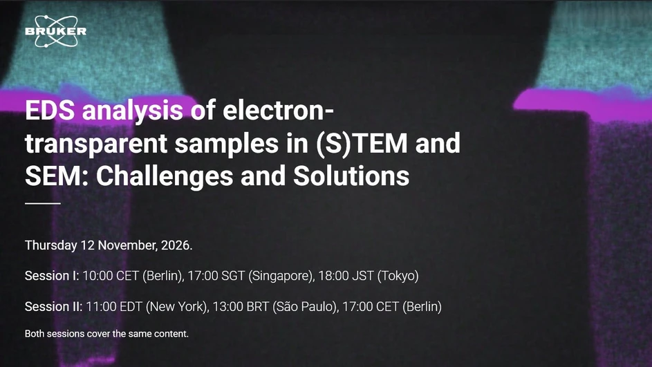
(S)TEM EDS provides powerful elemental information at high spatial resolution, but obtaining accurate quantitative results can be challenging when dealing with overlapping X-ray peaks, absorption effects, and complex nanoscale architectures.
Join this webinar to discover how Bruker’s latest (S)TEM EDS solutions help tackle these challenges and deliver reliable elemental characterization, even in the most demanding applications.
Through real-world case studies at both high and low accelerating voltages, we will demonstrate the characterization of nanometer-scale features and complex architectures, including advanced semiconductor devices.
Whether you work in semiconductor research, materials science, or nanotechnology, this webinar will provide practical approaches to improve the accuracy, reliability, and interpretation of your (S)TEM EDS data.
Join us and take the opportunity to discuss your applications and questions live with our experts during the Q&A session.
Speaker: Dr. Julien Aubourg (Application Scientist EDS, Bruker Electron Microscope Analyzers)
Speaker: Dr. Igor Németh (Application Scientist EDS, Bruker Nano Analytics)